

Key Takeaways
- Imec has fabricated 10 nm solid-state nanopores on full 300 mm wafers with high uniformity.
- The breakthrough leverages EUV lithography, a process typically used in cutting-edge semiconductor manufacturing.
- Results show a signal-to-noise ratio of 6.2, with the potential to push pore sizes below 5 nm.
- This achievement transforms nanopores from a lab-scale technique into a realistic mass-production platform.
- The CMOS-compatible design could enable high-throughput arrays for DNA sequencing, diagnostics, and data storage.
- Solid-state nanopores offer superior durability compared to biological nanopores used by companies like Oxford Nanopore.
Belgium’s leading semiconductor R&D center, imec, has reached a major milestone in the convergence of chip manufacturing and biotechnology. At the IEEE International Electron Devices Meeting in San Francisco, researchers announced the first successful wafer-scale fabrication of solid-state nanopores using the same EUV lithography tools used for cutting-edge computer chips.
Nanopores are nanometer-sized holes capable of detecting single molecules including DNA, RNA, and proteins as they pass through, generating measurable changes in ionic current. Although biological nanopores have already found commercial success in sequencing platforms, solid-state nanopores have long promised greater stability, better durability, and seamless integration with semiconductor processes. Until now, however, solid-state nanopores have struggled to achieve uniformity at commercial scale.
Imec’s demonstration marks a breakthrough. The team fabricated 10 nm pores across full 300 mm wafers, achieving consistent performance and a signal-to-noise ratio of 6.2, strong enough for sensitive molecular detection. With additional process refinements, the researchers believe they can reach pore sizes below 5 nm, enabling even more precise sensing.
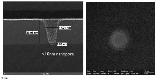
What makes the achievement especially significant is the use of EUV lithography, a highly advanced technique normally reserved for next-generation memory and logic chips. “We can apply EUV lithography to life sciences,” said Ashesh Ray Chaudhuri, imec R&D project manager and first author on the work. “This opens the door to high-throughput biosensor arrays for healthcare and beyond.”
By tapping into standard CMOS fabrication processes, imec’s technology could enable mass production of nanopore arrays for applications like personalized medicine, rapid infectious disease diagnostics, environmental monitoring, and even molecular-scale data storage. Solid-state nanopores not only withstand harsh environments better than biological pores, but they also integrate cleanly with semiconductor circuits, making them ideal for portable, low-cost devices.
Imec, headquartered in Leuven and employing more than 6,500 people, continues to expand its influence in both semiconductor and biotech innovation. With 2024 revenues exceeding €1 billion, the organization is well-positioned to accelerate the commercial transition of nanopore biosensors from research labs to real-world deployment.